South Korean team controls crystal growth in 2D chip materials
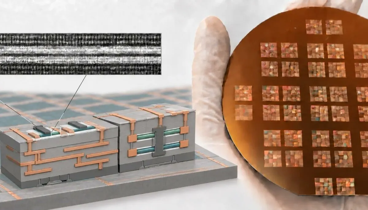
South Korean researchers have solved a key obstacle to manufacturing next-generation semiconductor chips at scale: controlling where 2D semiconductor crystals grow. Publishing their findings in Nature, the team from KAIST and startup TDS Innovation demonstrated a technique that ensures single crystals form precisely where needed, rather than haphazardly across a surface. Currently, random crystal formation creates boundaries that degrade electrical performance, but this breakthrough could unlock a new generation of more efficient chips.
The researchers used an etching flux, releasing oxygen from an oxide barrier to suppress crystal nucleation everywhere except at the geometric centre of patterned growth regions. Their EF-SCN process achieved a 99.3 per cent success rate across a two-centimetre substrate, producing single crystals at 397 of 400 patterned sites. The working transistors they built demonstrated higher charge-carrier mobility than previously achieved, and stacking these 2D materials onto silicon chips could bring logic and memory closer together, improving efficiency. Commercial use is targeted around 2030, with the team noting that AI demand could accelerate adoption.
- Researchers control 2D semiconductor crystal growth using oxygen-based etching technique
- Achieved 99.3 per cent success rate in trials on 2cm substrate
- Commercial production targeted for around 2030
New here? Start with this
Next-generation computer chips will need to handle more computing power whilst using less energy. Scientists are exploring new 2D materials—ultra-thin materials made from layers of atoms—as a potential solution. These could eventually replace or supplement the silicon materials used in today's chips.
The challenge with these materials is controlling how they grow during manufacturing. When grown in the laboratory, crystals form randomly across a surface, creating boundaries between different crystal regions. These boundaries weaken electrical performance, making the materials unsuitable for mass production.
A team of South Korean researchers has now demonstrated a technique to control exactly where crystals form during manufacturing, achieving extremely high precision. If the technique can be scaled up successfully, it could enable mass production of more efficient chips. The researchers expect commercial applications around 2030, with growing demand from artificial intelligence potentially accelerating development.
Read the full article at the source →
Originally published by The Register as “Researchers work out how to control 2D semiconductor growth for future chips”.